We need:
- transparent paper (for the exposuremaske)
- 6 x 10 cm photopositve material for the PCB (I'm strongly suggest to by more material, as we need. The first try is mostly a mistake - this was my experience.)
- a UV-lamp (a normal luminescence lamp will do it also)
- developer for the exposed PCB: NaOH
- caustics: FeCl3 or other
First:
The exposuremask must be printed to the transparent paper. That may be done with a normal black-white printer. The best results you will have with a laser-printer.
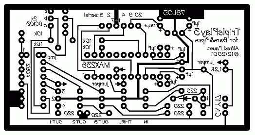
Please don't download and print this picture. I've made it smaller for the webpage. Please use the picture from the archive, which you may download --» here.
If you want to use a inkjet-printer, it is possible, that the black color is not real black. Than it may be, that there are some difficulties (see below). You can also make a fotocopy with maximum contrast. The result is like a printout with a laser-printer.
The #?.ps - files you can print out using "ghostscript" or "post", if you have no postscript-printer. Then all will be printed in the right messures.
The #?.gif - files you can print out with any graphic print program ("graphic-publisher" of "Turboprint", or "Studio" or other). A DTP-Program is also a good coice. You must experiment a little up to the measure-lines matchs the lenght that shown. A small difference of +/- 1mm doesn't matter.
NB.: With Multiview you can view the iff-pictures. Printing with Multiview is not so good.
I've made the PCB with ProDraw3. If you have this program, I can mail you the file. With this the printig is easier and accurate.
If you can't make PCB's by yourself, I can help you. But I'm not a electronic concern ... ;-)
I recommend you very much also printing out the TP3Plan.gif and the TP3Comp.gif. So you can always see what you do.
(Like above: Don't try to download and use these pictures. Please use the pictures from the downloaded archive.)
The plan is a mixed form for people, are not so familiary with circuitry.
Second:
Prepare the developer and the corrosivebath.
!!!! CAUTION !!!
The developer and the corrosive are very corrodive.
!!!! USE GLOVES !!!
NaOH : 50g to 1l water
FeClł: 400g to 1l water
Lay the printed mask down the PCB-material. (remove the protectionsfoil before). Use the mirrored one with the printcoulor to the PCB. That means, that it is now unmirrored. Press it down with a glasplate. Than lay it under the UV-lamp.
exposure time with UV-lamp : 3 min
exposure time with flourecent-lamp : 7-8 min
(a small distance between lamp and PCB is necessary)
After the exposure put the PCB immediately in the developer. In a short time you will now see appearing the line wires. When all spaces between the line wires are free, immediately take the PCB out of the developer and bring it under water. Then let it dry accurate. Don't use a cloth, it wipes the line wires.
NB.: I tryed to make the mask with a inkjet-printer. The ink isn't real black. So the UV-light wasn't exact shielded at the black lines. So the developer also destroyed the lines and the PCB was lost.
So I experimented a little. My result:
Make a low concentrated developerbath : 20g NaOH to 1l water
Print the exposure mask at normal Inkjet-paper.
Exposure like above explained.
Lay exposured PCB with the metal side to top in the developer bath. Wait so long up to all lines are clearly to see. (the color of the parts, that will later cauterized changed to blue.) Then immediately put it under flowing water.
You can put the PCB again in the developer if it is not enough developed, and than again under the water .... and so on. You can also hold down the PCB partially in the developer bath.
Be careful ! In the other way you will lose your work.
But this is only for that reason if you use a inkjet-printer.
If the PCB is dry, put it in the corrosivebath . The time it takes to cauterize is between 10 min and some hours. Look often at the PCB in the corrosivebath. If you heat up the corrosivebath to 60°C the cauterize-time will be very short. Often move your PCB in the bath, that will also minimize the time.
If all line wires clean cauterized, put the PCB under water to wash up all corrodive thorough.
Third: Drilling:
- use a drill 0,8 - 1,0 mm thick.
Forth: Soldering:
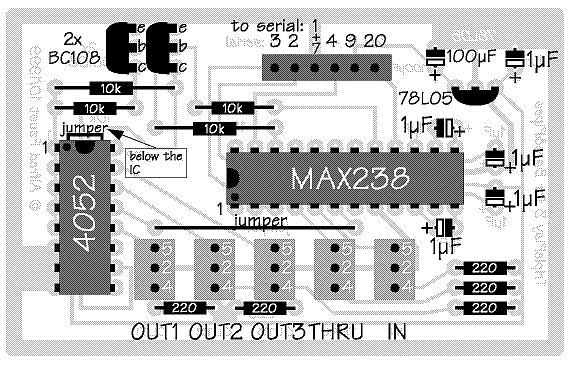
Print out the TPP3Components.iff. So you can see in the right form, how to build in the components.
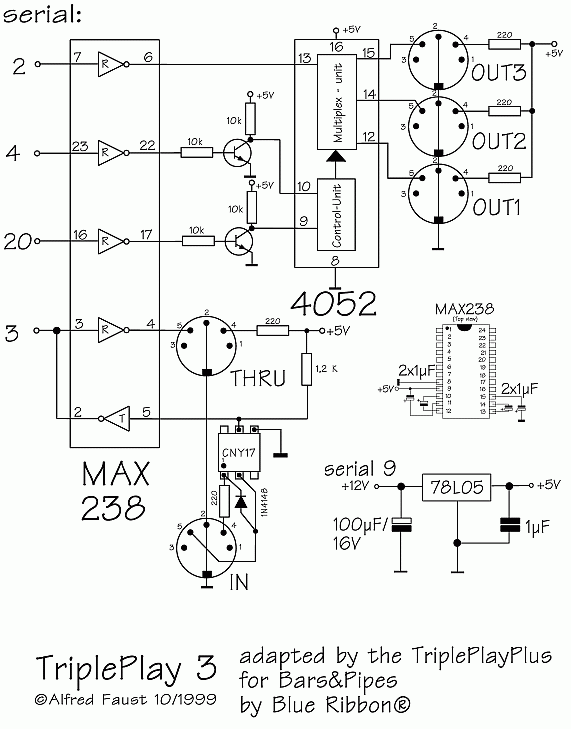
Also at the PCB you can see how all components shall be connected. Also you will see the connections to the PCB. (MIDI-Output, and serial connection)
Use a electric soldering iron with no more than 20 W.
Look accurate before soldering the IC.
I'm very recommend to use sockets for the IC's. They are very cheap, and if anything is wrong, you must not dissolder the IC - this is very difficult.
                     ___   ___
                 1 =|    O    |= 16
                   =|         |=
                   =|         |=
                   =|   4052  |=   Top View
                   =|         |=
                   =|         |=
                   =|         |=
                 8 =|_________|= 9


                     ___  ____
                 1 =|    O    |= 24
                   =|         |=
                   =|         |=
                   =|   MAX   |=   Top View
                   =|   238   |=
                   =|         |=
                   =|         |=
                   =|         |=
                   =|         |=
                   =|         |=
                   =|         |=
                12 =|_________|= 13
Use only so much solder tin as necessary. Use only solder tin for
electronics.There a long jumper to sold in. At the PCB these are marked with "jumper".
Don't forget these! I recommend to use a isulated wire.
For the MIDI-Ports use normal DIN-sockets:
View from the back (soldering) - side:
                -------------
               |             |
               |      2      |
               |   5     4   |
               |  3       1  |
               |             |
               |      S      |
               |             |
                -------------
S = Shield of the Plug (must be connected to Pin 2)You also can see this at the plan.
Most there are numbers of the pins at the DIN-sockets. Look accurate please.
For the connection to the DIN-sockets use soldering pins, or sold in PCB-plugs.
The numbers of the pin-connections of the serial-port-plug you see at the top of the PCB.
3 2 1/7 4 9 20 CONNECT ONLY THIS PINS. THE PIN 1 + PIN 7 MUST BE CONNECTED AT THE SERIAL-PORT-PLUG !!!
DON'T CONNECT THE SHIELD AND PIN 1 + 7.
CONNECT THE SHIELD SEPARATLY BESIDE THE PINS.
LOOK VERY ACCURATE AND COUNT THE PINS FOR SECURITY THREE TIMES ORE MORE.
MOST FOR PIN 9 and 10.
THE REASON IS:
PIN 9 HAVE +12V
PIN 10 HAVE -12V !
IT WILL BE VERY DANGEROS IF YOU EXCHANGE THESE TWO PINS. THE IC's WILL BE DAMAGED.
At last build the PCB and the DIN-sockets in the metal case. For the connection to the serial-port I made a short cable with the female plug at the one side.
Before you connect or disconnet to your AMIGA:
!!!!! S W I T C H O F T H E P O W E R !!!!! IT IS VERY EASY TO DESTROY THE PORT IC's, WHEN YOU MAKE ANY CONNECTION OR DISCONNECTION AT YOUR AMIGA, IF THE POWER IS ON.
The time you loose with a new boot is very good invested in the life of your AMIGA.
BE WARNED ....
And now good luck and many fun with the Triple-Play-MIDI-Interface .... :-))